Advanced equipments to create smart and efficient work environments

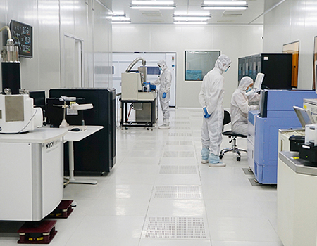
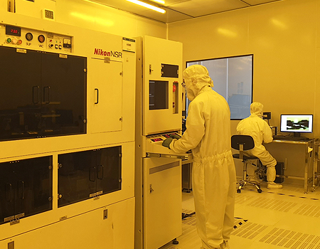
Aosong Electronic has advanced MEMS semiconductor smart sensor feature chip production line, which is equipped with 100-level clean photolithography area, 1,000-level clean coating area, etching area, ion implantation area, wet cleaning area and visit channel, etc., and introduced a number of advanced semiconductor high-end equipment, with high-end feature chip R&D and customization capabilities is the Guangdong, Hong Kong and Macao Greater Bay Area advanced MEMS semiconductor chip manufacturing enterprises.
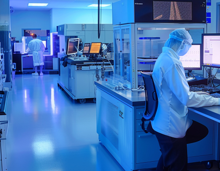
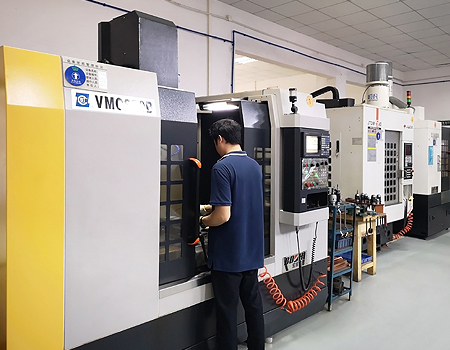
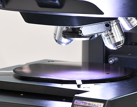
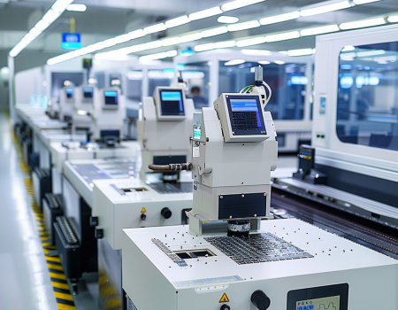
In 2021, Aosong Electronic invested a lot to upgrade the MEMS wafer-level advanced packaging production line to create a dust-free and clean workshop with international first-class packaging equipment such as laser invisible cutter, lobe machine, solid crystal machine, wire bonding machine, A01, SMD machine, plastic sealing machine, X-RAY, and so on. The advanced packaging technology greatly improves the chip performance and meets the demand for MEMS sensor chip performance, power consumption, quality, cycle time and cost.
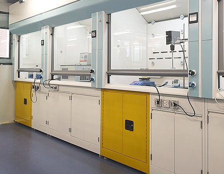
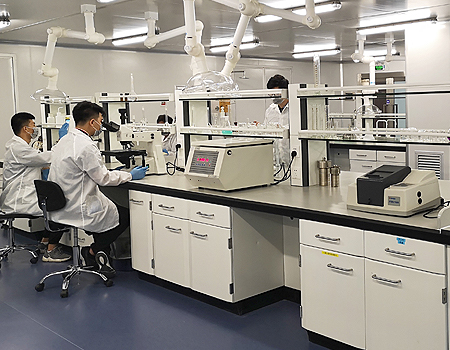
With the goal of opening up the complete innovation chain of raw materials-products-applications, Aosong focus on research in the directions of electronic information materials, new energy raw materials, advanced polymers and composites green chemical industry and high-end chemical materials, accelerating the process of domestic substitution, and steadily improving the performance of intelligent sensor products.